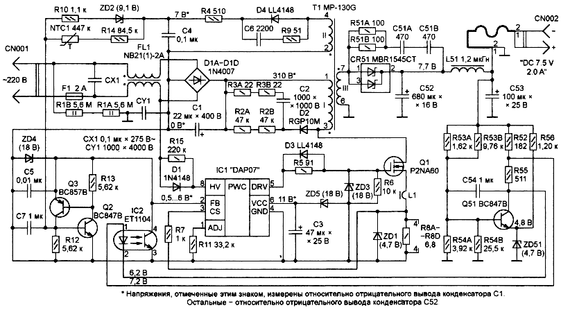
Psone Schematics.

Argelfraster

Well-Known Member
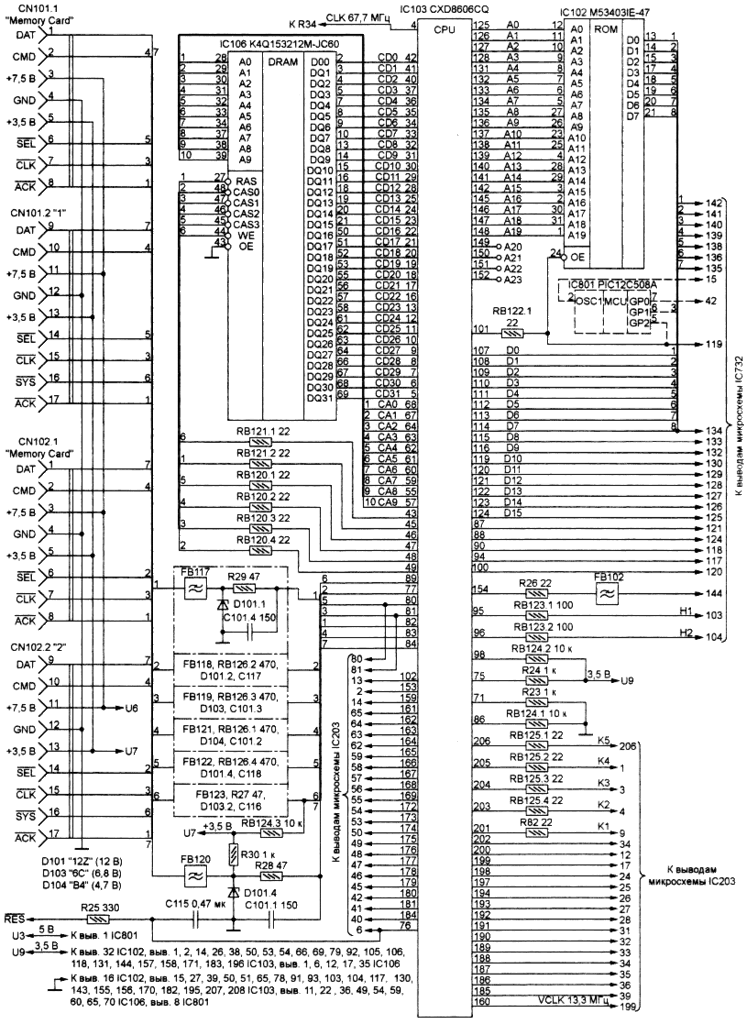
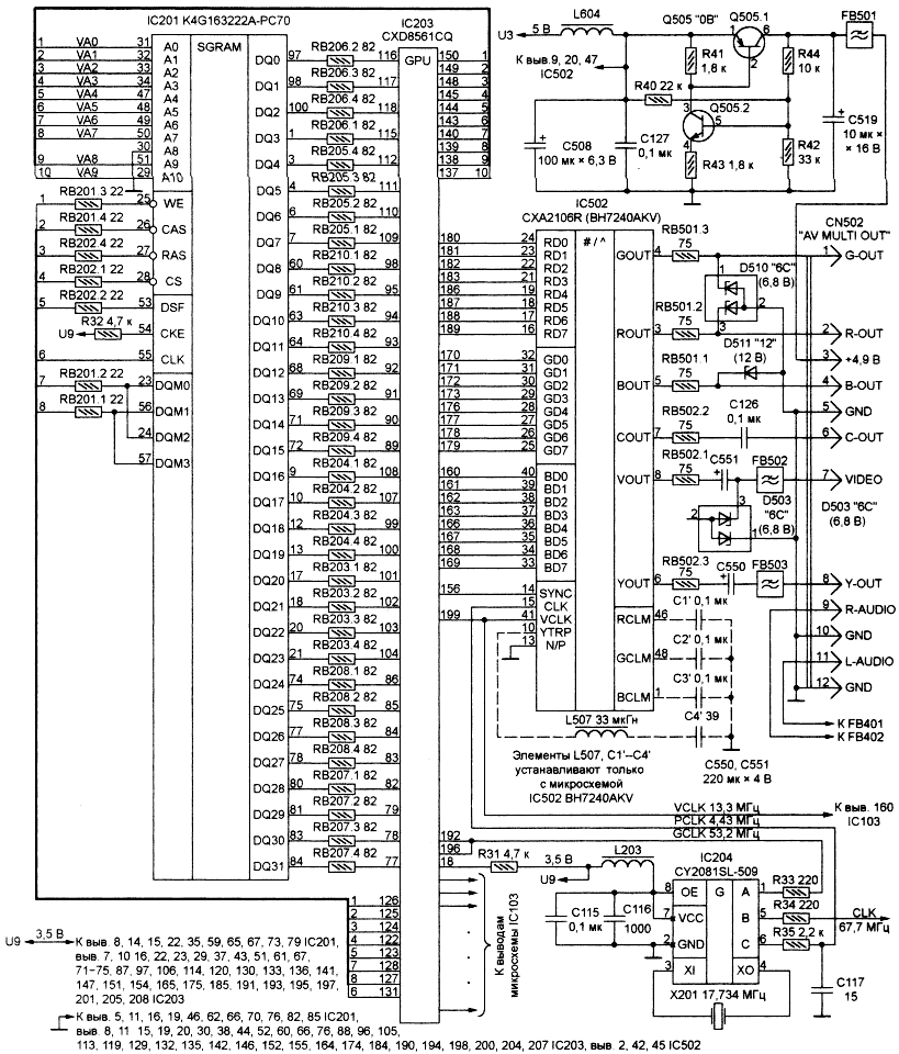
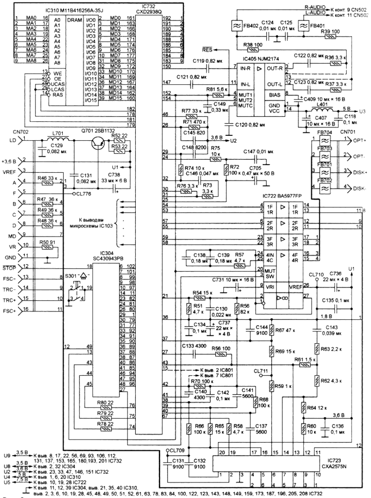
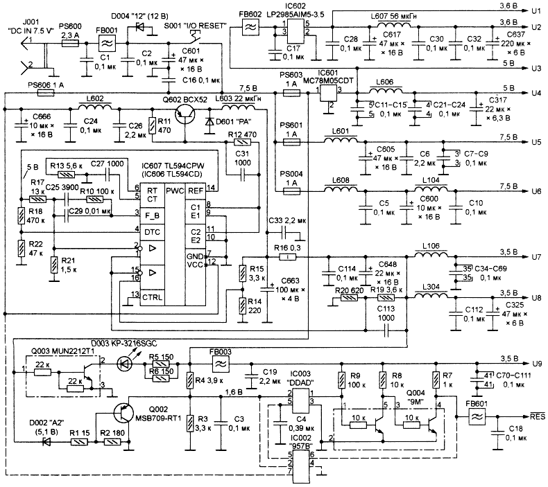
I believe these are PSone schematics. :D
1.gif

2.gif

3.gif

4.gif

5.gif
 
Can't tell, but they certainly look complex enough.

Diggin' the Russian/Cyrillic at the bottom. Boris probably ripped it off and posted it.
 
If you sent 'em to a PCB fabrication company, had it designed for you, and had a ton of monies, yes.

If you made a 6-layer board, it could get pretty small...
 
Not quite sure how that works.
Is there a way to give them the schematics and then they tell you how much it is before you buy it?
 
Sunstone does NOT design PCBs, they manufacture them.

If you want to use those schematics, you're going to need someone who can work with them and create a set of Gerber files.
Plenty of software out there, even free, that you can use that for.

From there, you'd need to send it to a PCB Manufacturer, and trust me, even a 2 layer board would be expensive.
If you want to make it SMALLER than the PSOne board, you'd be looking at a 4 - 6 layer board, and many hundreds of dollars.
 
Argelfraster said:
There's no way to figure out how to make an OAC?

What, from this?
No.
These are just wiring schematics, the kind you'd use to make a PCB.

These don't include any information about the ICs used, such as the actual Processor, etc.
 
Why bother? The PCB is already really small, and making it smaller would require a skilled person with a lot of time, it would be expensive, and you probably wouldn't gain that much.

I'd be more interested in redesgined, thinned out drive units for disc-based systems myself.
 
XCVG said:
I'd be more interested in redesgined, thinned out drive units for disc-based systems myself.

I'd be more interested in a drive emulator, which loads ISOs off of an SD card into a RAM Drive in place of the existing disc drive.
 
Haunted360 said:
Yea, those are 100% PlayStation.


See how the Information Controller's (Chips) are labeled IC102?

IC102 is the Boot ROM IC.
Are you going to bump every topic in the Psone section?
 
Back
Top